
A University of Illinois team has stacked working layers of single-crystalline silicon directly on top of finished circuits using a bonding step that never climbs past 200 degrees Celsius, roughly half the 400-degree ceiling that has blocked true monolithic 3D integration for years. The method, reported in the journal Nature, delivered device yields of 98 to 100 percent across the stacked layers, the kind of number a chip foundry wants to see before it touches a new process.
The catch is distance. A three-layer demonstration carrying 625 transistors per layer sits a long way from a production line, and the companies that would actually build it, IBM, Intel and Taiwan Semiconductor Manufacturing Company, already have their own stacking bets running.
The 400-Degree Wall That Stopped Stacking Silicon
Making high-quality crystalline silicon and the transistors that live in it normally calls for heat approaching 1,000 degrees Celsius. That is fine for the very first layer of a chip. The trouble starts once that layer carries metal wiring, because the same temperatures that grow good silicon would cook the interconnects already sitting underneath.
So the industry settled on a rule. Once the bottom circuits are done, anything stacked above them has to be built under a thermal budget of about 400 degrees, the point past which existing metal lines start to degrade. For years that limit pushed researchers toward exotic upper-layer materials, polycrystalline silicon, amorphous metal oxides, carbon nanotubes, two-dimensional semiconductors, each of which traded away performance or reliability against the silicon in the bottom layer.
The Illinois group went the other way and kept the silicon. Its process peels ultrathin freestanding silicon nanomembranes, 10 nanometers thick or less, off a donor wafer and lays them onto a substrate that already holds completed circuitry, using a roll laminator that tops out at 200 degrees. Because the films are so thin, they bend to fit the surface below, conforming closely enough to dodge the voids and interfacial defects that wreck rigid wafer-to-wafer bonding. The payoff turned up in the yield figures.
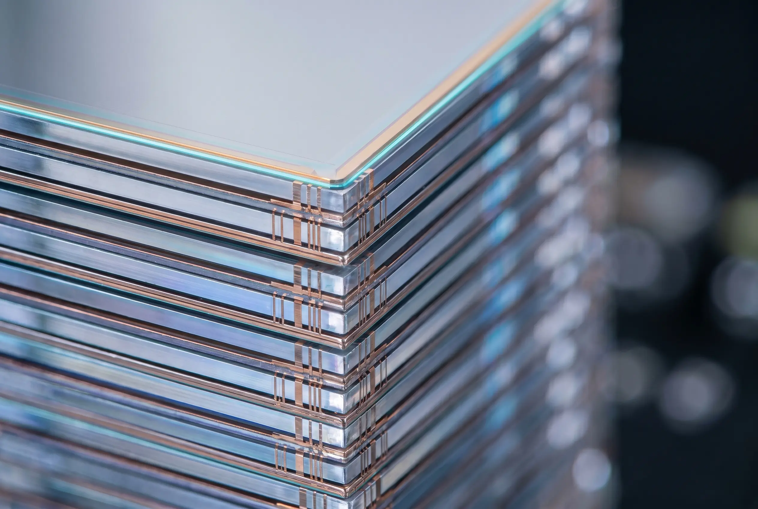
From Six Transistors on One Floor to Six Across Several
Why bother building up at all? Density is the obvious answer, but speed and power matter more for the chips that feed artificial intelligence. Stacking shortens the wires between parts of a circuit, which cuts parasitic capacitance and widens the bandwidth between layers, and that interlayer bandwidth is exactly the bottleneck that throttles memory-hungry AI workloads.
Take static random-access memory (SRAM), the fast on-chip memory wired into every CPU and GPU. Storing a single bit takes six transistors sitting side by side on one plane. Spread those six across several stacked layers and the same cell eats far less floor space while the parts talk to each other over shorter, faster paths.
It’s like replacing a sprawling suburb with high-rises: you get the same functionality, but the spatial footprint is reduced while making communication between layers faster and more efficient.
That is Qing Cao, the materials science and engineering professor at the University of Illinois Grainger College of Engineering who led the work, describing the idea in plain terms. The vertical move buys back area without asking the transistor itself to shrink, and shrinking is the part that has gotten brutally hard. You can read more about Qing Cao’s materials science group at Illinois and its focus on nanoelectronics on the university’s own pages.
Why Glued Wafers Hit a Ceiling Monolithic Layers Don’t
Commercial 3D chips already exist, but almost all of them are glued together. Makers build devices on separate wafers, finish each one, then bond the slabs and link them with through-silicon vias (TSVs), the wide vertical channels that pass signals between layers. High-bandwidth memory and AMD’s 3D V-Cache both work this way, and both ship in volume today.
The limitation is resolution. Bonded wafers align coarsely, and TSVs are large and spread thin, so the count of connections between layers stays modest. Monolithic integration builds each new layer on top of the last instead of marrying two finished slabs, which lets the vertical links shrink and multiply. Researchers estimate the approach can raise interlayer connectivity by 10 to 100 times over conventional stacking, with alignment measured in nanometers rather than micrometers.
| Attribute | Wafer-bonded 3D | Monolithic 3D |
|---|---|---|
| How layers join | Finished wafers bonded together | Each layer built on the one below |
| Alignment accuracy | Coarse, micrometer scale | Nanometer scale |
| Vertical connections | Large, sparse TSVs | Dense, fine interconnects |
| Interlayer connectivity | Baseline | 10 to 100 times higher |
| Status today | Shipping (HBM, 3D V-Cache) | Lab demonstration |
That connectivity gap is the entire reason engineers keep chasing monolithic stacking despite its difficulty, and it is why a 200-degree result counts for something well beyond one campus.
Junctionless Transistors and the 625-Device Test
Holding the heat down meant rebuilding the transistor too. Conventional devices lean on doping, the deliberate addition of impurities that controls how silicon conducts, and the step that locks those impurities in place usually runs above 600 degrees Celsius. That single step would blow the thermal budget on its own.
The team’s workaround was the junctionless transistor. Here the silicon is doped uniformly and heavily before any stacking starts, so no high-temperature activation is needed once the layers are down. The films are thin enough that the gate still switches the current cleanly, and the heavy doping trims the parasitic contact resistance that normally drags on performance. It is a design that fits the constraint rather than fighting it.
- 98 to 100 percent device yield across the stacked silicon layers.
- 625 transistors per layer, repeated across three stacked layers.
- Output current density matching ordinary transistors built on bulk wafers at far higher temperatures.
- Three to four times better performance than monolithic devices made from alternative materials, such as the 2D semiconductors others have used for growth-based monolithic 3D stacking.
Across all three layers the devices behaved consistently, and the group wired the layers together to run real 3D logic circuits and SRAM cells rather than isolated test structures. That last point is what separates a curiosity from a process: the parts worked together, stacked, the way a chip block would.
Why the Industry Is Building Up Instead of Shrinking
For about 60 years, Moore’s law set the tempo of the chip business: transistor density on an integrated circuit roughly doubles every two years. It held for a remarkably long stretch, and it is now running into a wall that no clever floor plan can move.
Where Silicon Runs Into Physics
The squeeze is physical. “In a sense, we’re hitting a limit imposed by physics,” as Cao put it. Transistors have largely stopped shrinking in contacted gate pitch, the spacing that actually decides how tightly they pack, because silicon’s own material properties and the rules of quantum mechanics get in the way at atomic scale. Push the features closer and electrons start tunneling where they should not, leaking current and burning power for nothing. The old lever, shrink the device, is mostly tapped out, a slowdown that bodies like the research institute imec’s analysis of Moore’s law limits has tracked for more than a decade.
The Stacking Race Already Under Way
That is why every major maker is reaching for the third dimension. At the IEDM conference in late 2025, TSMC demonstrated a working 101-stage 3D monolithic complementary field-effect transistor (CFET) ring oscillator and the smallest SRAM bit cell yet shown. IBM and Samsung have demonstrated their own monolithic stacked transistor, and imec pencils in wide CFET production somewhere around its A5 node near 2032. The Illinois result lands in that same race, with a different bet: keep standard silicon on every floor instead of swapping in weaker materials up top.
The Lab-to-Fab Gap Cao Still Has to Close
For all the strong numbers, this is still a proof of concept. A real processor packs billions of transistors; a layer here holds a few hundred. The Nature paper shows the method works and behaves predictably, not that a foundry can run it at volume next quarter.
What the team is really selling is the slope. By its own account the process keeps yielding high-performing, low-variability transistors as layers pile up, so stacking past three becomes repetition rather than reinvention. That scalability claim is the reason the work is now pointed at an industrial foundry for its next trial, the step where most promising lab processes either scale or quietly die.
The institutional muscle is already lined up. The research ran through Illinois Grainger Engineering’s Center for Advanced Semiconductor Chips with Accelerated Performance, whose industry partners include IBM, Intel and TSMC, with funding from the National Science Foundation research programs and the Silicon Crossroads Microelectronics Commons Hub. That roster matters, because the same firms shipping wafer-bonded 3D today are the ones who would have to adopt the monolithic version tomorrow.
If the next demonstration carries a real circuit block through a foundry’s process flow, monolithic stacking stops being a paper and starts being a manufacturing option. If it stalls at the bench, the glued wafers that already ship keep the floor they have held for a decade.