
Applied Materials and Ushio have announced a breakthrough in digital lithography technology that will enable more powerful computing systems for the AI era. The new technology will reduce the cost, complexity, and environmental impact of advanced chipmaking.
What is Digital Lithography Technology?
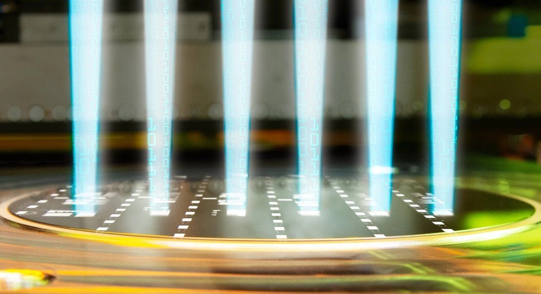
Digital lithography technology is a process that uses a laser to create patterns on a silicon wafer, which are then etched into the chip. The patterns define the features and functions of the chip, such as transistors and interconnect wiring. The smaller and denser the patterns, the more powerful and efficient the chip.
Why is it a Breakthrough?
The current state-of-the-art technology for creating small and dense patterns is called EUV lithography, which uses extreme ultraviolet light to project the patterns onto the wafer. However, EUV lithography has some limitations, such as the resolution limit, which means that some patterns are too small to be printed with EUV. To overcome this, chipmakers use a technique called EUV double patterning, which splits a high-density pattern into two masks that are printed separately and then combined on the wafer.
While EUV double patterning is effective at increasing the pattern density, it also adds design and patterning complexity, as well as process steps that consume time, energy, materials, and water. This increases the cost of wafer fabs and wafer production, as well as the environmental impact of chipmaking.
The breakthrough digital lithography technology from Applied Materials and Ushio provides a simpler, faster, and more cost-effective alternative to EUV double patterning. The technology, called Digital Lithography Technology, allows chipmakers to print a single EUV pattern and then use a system called Centura Sculpta to elongate the shapes in any chosen direction to reduce the space between features and increase pattern density. This eliminates the need for a second mask, as well as the alignment errors and extra process steps associated with EUV double patterning.
What are the Benefits?
According to Applied Materials, the benefits of using Digital Lithography Technology instead of EUV double patterning are significant. For each EUV double patterning sequence it replaces, the technology can provide chipmakers with:
- Capital cost savings of approximately $250 million per 100K wafer starts per month of production capacity
- Manufacturing cost savings of approximately $50 per wafer
- Energy savings of more than 15 kwh per wafer
- Direct greenhouse gas emissions reduction of more than 0.35 kg of CO2 equivalent per wafer
- Water savings of approximately 15 liters per wafer
The technology can also reduce the design cost and complexity, as well as the yield risk, by using a single mask instead of two. Moreover, the technology can enable more powerful and efficient chips for the AI era, as it can create smaller and denser features and functions on the chip.
How Does it Work?
The Digital Lithography Technology consists of two main components: the Centura Sculpta patterning system and the Ushio lithography system. The Centura Sculpta patterning system is a new product from Applied Materials that uses a laser to shape the patterns on the wafer. The system can elongate the shapes in any direction, such as horizontal, vertical, or diagonal, to create the desired pattern density. The system can also create complex shapes, such as L-shapes, T-shapes, or S-shapes, to optimize the chip performance and functionality.
The Ushio lithography system is a product from Ushio, a Japanese company that has over 20 years of experience in building lithography systems for packaging applications. The system uses a laser to print the single EUV pattern on the wafer, which is then shaped by the Centura Sculpta system. The system can print patterns with a resolution of 1.5 microns, which is sufficient for the initial EUV pattern.
The combination of the Centura Sculpta and the Ushio lithography systems creates a new digital lithography technology that can produce high-performance and low-cost chips for the AI era.
What are the Applications?
The digital lithography technology can be applied to various types of chips, such as logic, memory, and interconnect. The technology can create smaller and denser transistors, which are the basic building blocks of logic chips. The technology can also create smaller and denser interconnect wiring, which connects the transistors and other components on the chip. The technology can also create smaller and denser memory cells, which store and retrieve data on the chip.
The digital lithography technology can enable more powerful and efficient computing systems for the AI era, as it can increase the performance, functionality, and capacity of the chips. The technology can also enable new applications and innovations in fields such as cloud computing, edge computing, 5G, autonomous vehicles, and smart devices.
What are the Challenges?
The digital lithography technology is a new and innovative technology that requires collaboration and coordination among various stakeholders, such as chipmakers, equipment suppliers, and materials suppliers. The technology also requires rigorous testing and validation to ensure its reliability and quality. The technology also faces competition from other emerging technologies, such as nanosheet transistors, 3D stacking, and neuromorphic computing, that aim to improve the chip performance and efficiency.
The digital lithography technology is a breakthrough in chipmaking that will enable a new era of computing power for the AI era. The technology will reduce the cost, complexity, and environmental impact of advanced chipmaking, while enabling more powerful and efficient chips for various applications and innovations.